High throughput laser passivation tools
Passivation of laser facets
Passivation of compound semiconductors
Surface passivation
Surface passivation is an important step in semiconductor processing. For instance, in laser diode manufacturing, it prevents potential damage or even destruction of the laser. Different coating methods can be used to protect surfaces or facets: ZnSe, SiN, oxides. Our CPS reactor is designed to provide effective passivation based on strict process conditions to ensure stability, reproducibility, control of the coating.
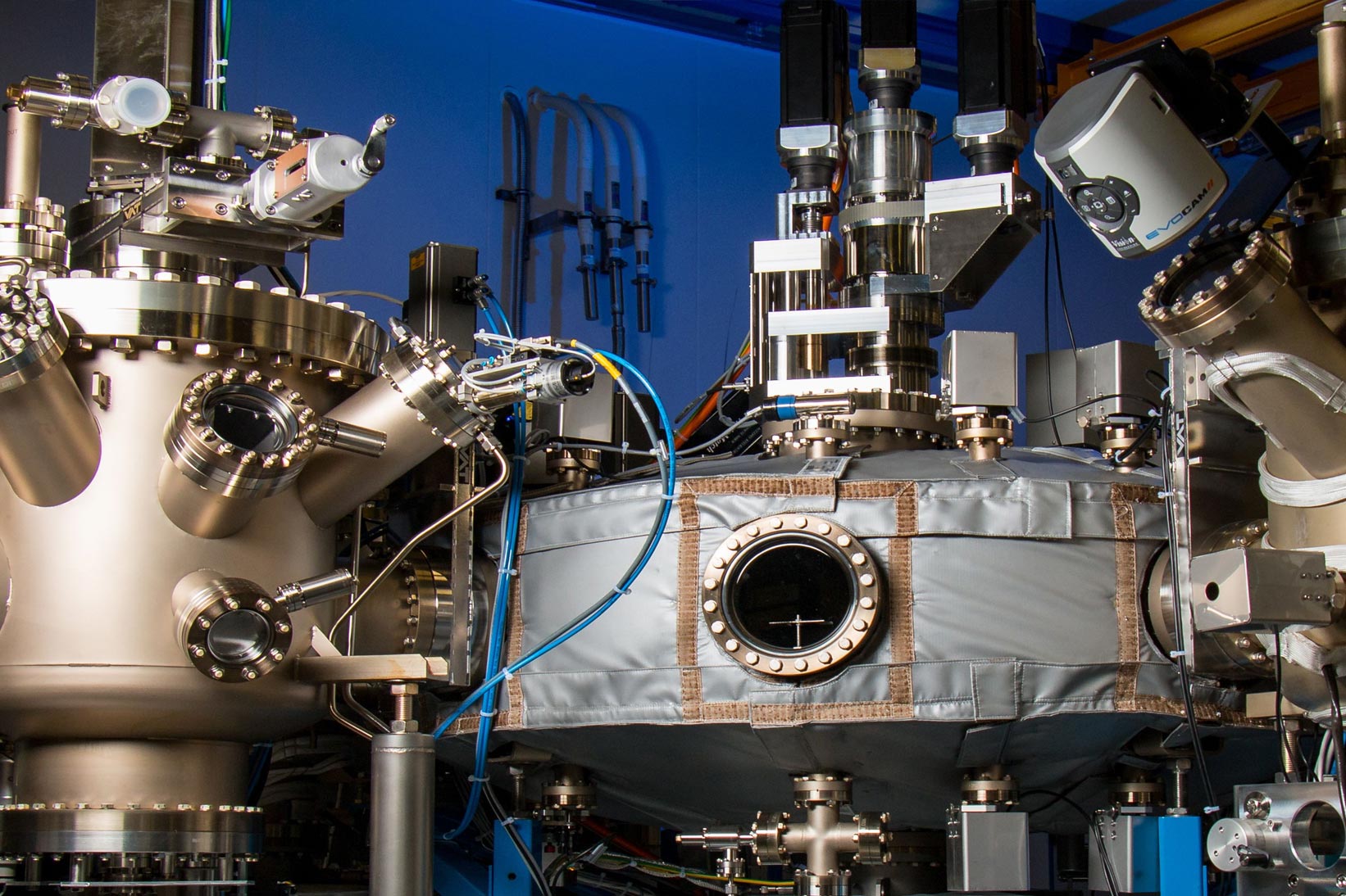
CPS reactor specifications
 Up to 5 devices loaded at once
 Fully automated system
 Riber CrystalXE – www.crystalxe.com
UHV reactor to prevent contamination
- Dedicated vacuum pumps and cooled panels
- Ultimate pressure <5.10-10 Torr
Perfect control of the deposition
- Stable, reproducible and uniform material sources
- Valved cell, Oxygen or nitrogen plasma, Si gas injector
- Low temperature (typ. 200-400°C) rotating heater
In-situ metrology tools for precise control of the layer stoichiometry and thickness
- RHEED
- Quartz crystal sensor │ellipsometry (on request)
- Temperature
Smart control
- Fully automated reactor
- Optimized timeline
- Automatic calibration steps
- Access to all parameters at anytime
Flexible and expandable reactor
- Modular configuration based on a cluster
- Easy-to-integrate third parties’ instrument
CRITICAL SURFACES CLEANING
Any surface exposed to air will experience uncontrolled oxidation to some extent. For example, cleaved lasers facets are exposed to oxidation. This native oxide limits the maximum output power and device lifetime.
The Riber CPS system includes a cleaning chamber in which troublesome oxides can be removed by a thermal desorption process enhanced by exposure to a hydrogen plasma source resulting in a pristine damage-free underlying compound semiconductor surface.
Cleaning chamber specifications
Independant UHV reactor connected to the CPS reactor
- Dedicated vacuum pumps
- Ultimate pressure <5.10-10 Torr
Native oxide removal
- Low temperature (typ. 200- 400°C) rotating heater
- Hydrogen RF plasma source
In-situ metrology tools for process control
- Crystal quality : RHEED
Flexible configuration
- Up to 3 source ports
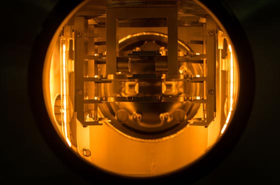
DELIVERING SUPERIOR LAYER INTERFACE QUALITY
By performing the surface cleaning and passivation process entirely under UHV conditions, an extremely high quality and clean passivation layer interface is achieved.
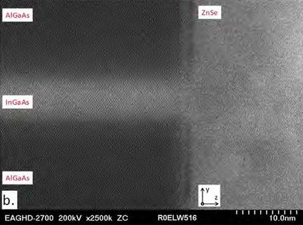
XSTEM image of the 3D epitaxially grown semiconductor. The AlGaAs waveguide layer and InGaAs quantum well were grown by MOCVD. ZnSe passivation layer deposited in the CPS reactor (MBE412) with growth in direction z.
3D grown epitaxial semiconductor displays clearly resolved & defect free lattice sites.
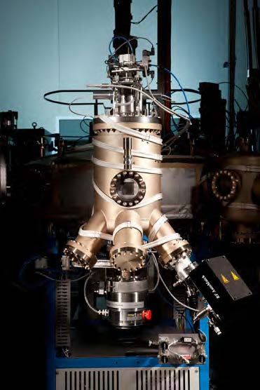
CPS CONFIGURATION
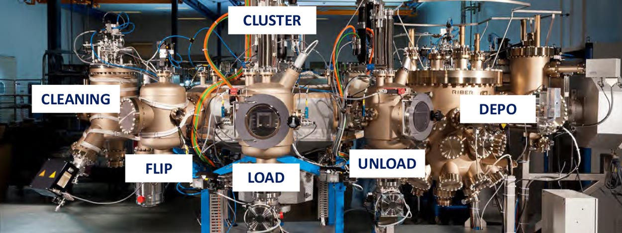
Multi-chamber UHV CPS is configured with different chambers specifically designed for different aspects of surfaces or laser facet passivation.
The devices are transferred from chamber to chamber under UHV conditions to ensure surface cleanliness is maintained throughout the process. This example includes the capability to flip the device holder in both sides of the lasers to be cleaned and passivated.
Depending on customer yield requirements and process timeline, additional process chambers can be added to the system.