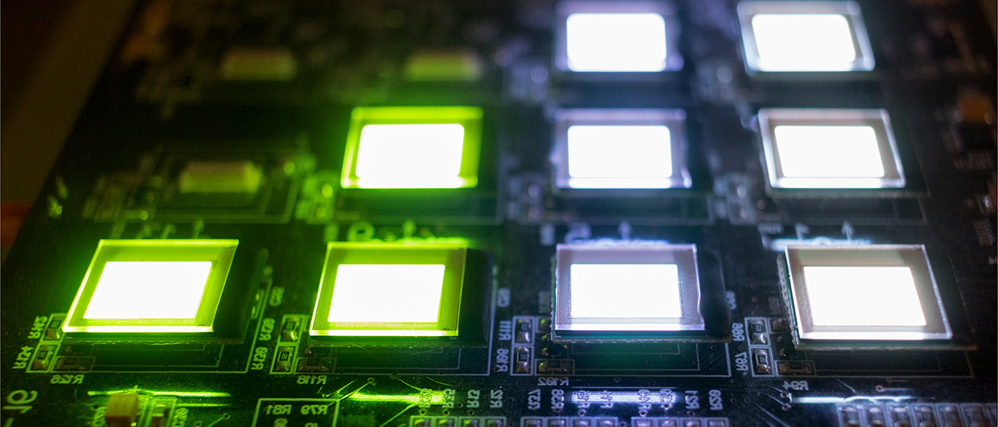
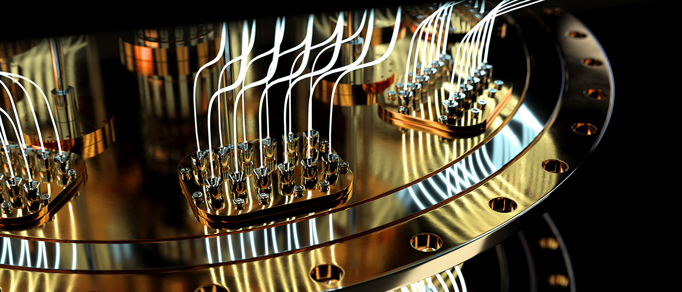
Innovative solutions for semiconductor industry
News & Events

Products
-
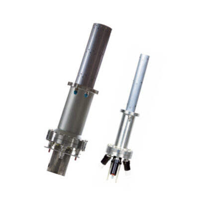
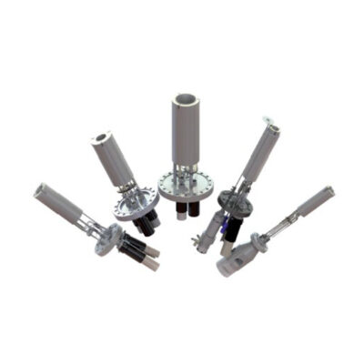 In & Ga Graphite-crucible cells for Nitrides - MS
-
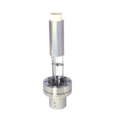 Aluminum source ABN BF CL & CN
-
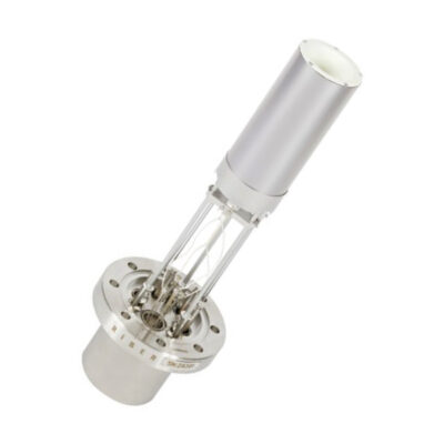 Dual filament source - ABN DF
-
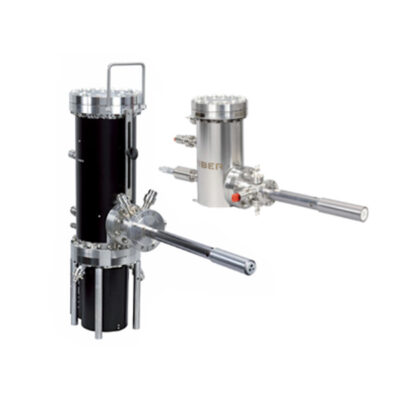
 Valved Source for Corrosive Materials - VCOR
-
 Valved Cracker Cell for Arsenic - VAC
-
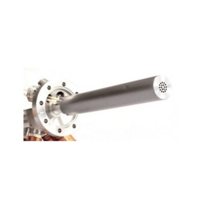 LTI – Low Temperature Injector
-
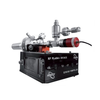 RF Plasma Source for Hydrogen - RF-H 600
-
Versatile valved Source
-
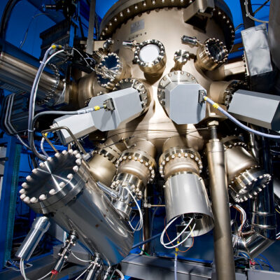 MBE 49 - 5x3’’, 4x4’’, 150, 200mm production system
What we do
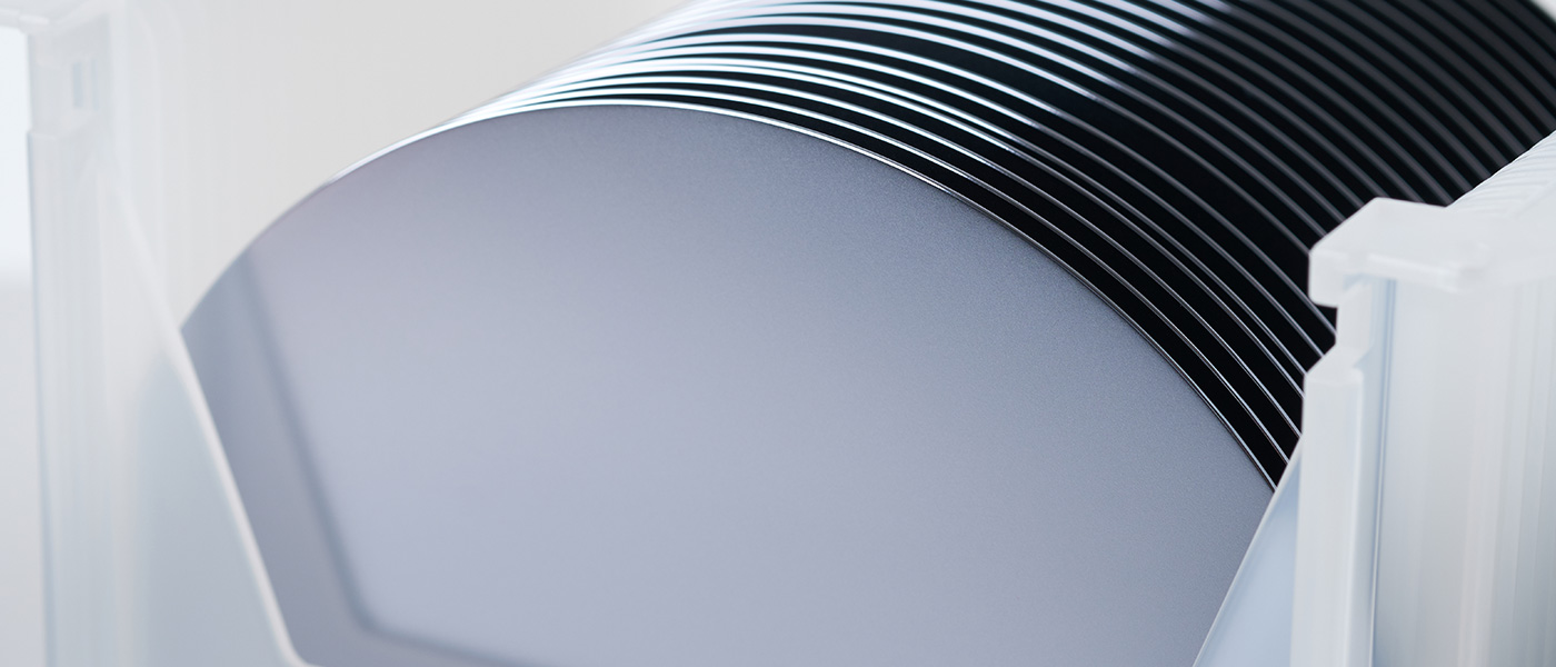
About MBE
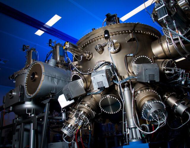
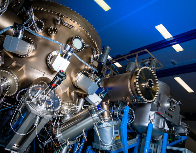
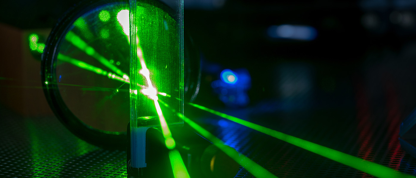
At the heart of every LED, laser diode, solar cell and transistor is a stack of semiconductor layers, each with a carefully controlled composition, thickness and electrical conductivity. To ensure optimal device performance, these layers must be deposited in a carefully controlled manner, layer of atoms by layer, to form complex structure featuring light or waves adapted to the needs and not achievable with common silicon technology.
MBE is the ideal growth technology for depositing films in this manner. This growth technique generally uses several solid or gaseous elements which are heated and sent onto the substrates to form layers of the right composition, thickness and doping. These layers are arranged in sequences to form the desired structures for the application or research purpose.
The uniqueness of MBE is to be able to deposit thin layers of atoms with an incredible thickness resolution (a monolayer), a superb uniformity, cleanliness and reproducitility. Riber provides the broadest line of innovative and high quality molecular beam epitaxy (MBE) systems designed for each main lines of compound semiconductors: III-V, Gallium Nitrides, II-VI and MCT, SiGe and new materials such as Graphene.
Who we ARE

Riber operates in a specific domain: we are experts in Molecular Beam Epitaxy (MBE), a technique which is used to grow compound semiconductors, and we provide Innovative Solutions for Semiconductor Industry.